| The Following User Says Thank You to joerg_rw For This Useful Post: | ||
|
|
2013-11-24
, 15:20
|
|
|
Posts: 2,222 |
Thanked: 12,651 times |
Joined on Mar 2010
@ SOL 3
|
#1342
|
To give you some insight into our work and the progress we make.
Some photos of the mech-validation PCBs:
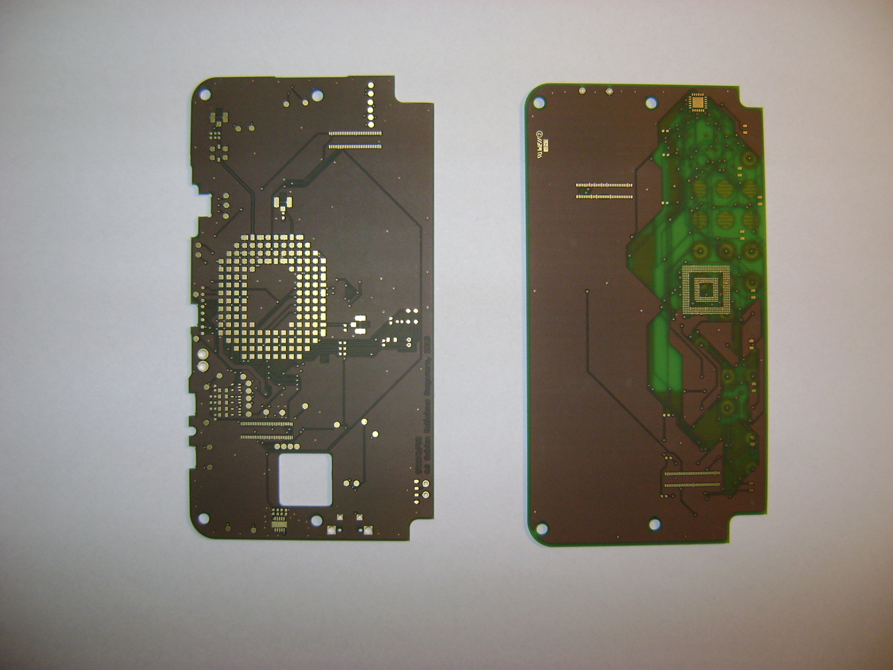
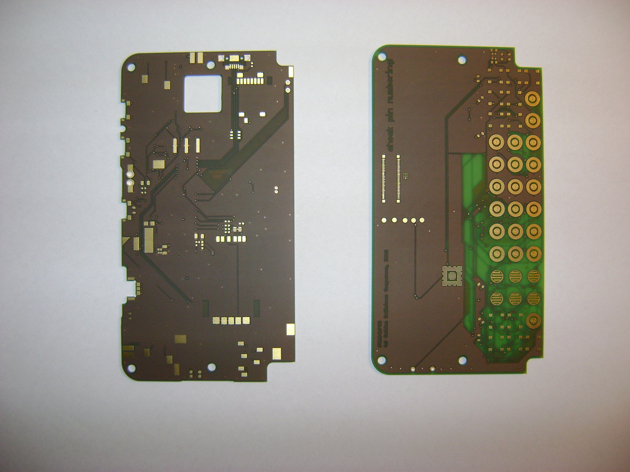
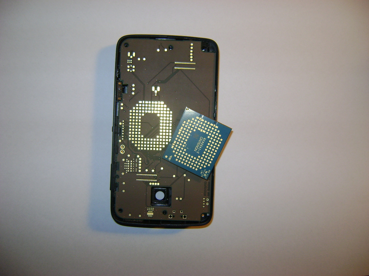
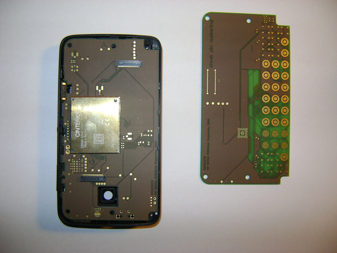
More of those (in highres) on the GolDeliCo download site.
/j
Last edited by joerg_rw; 2013-11-24 at 18:35.
Kommentare (neueste zuerst):
# Von Nikolaus Schaller, Nov 24, 2013:
More observarions:
* LOWER: PCB snaps nicely into snap-fits and cutout between + and - buttons is very good
* but mounting holes are not exact enough
* LOWER: mounting holes for USB connector are muchtoo big (radius vs. diameter?)
* LOWER: position of ON-Key appears to be weird compared to button on case, but fits exactly to PCB
* LOWER: Camera hole appears still to be deplaced by 0.1-0.2mm and needs to be drilled in the corners before milling
* LOWER: Pogo-Pins are not well centered where they should be, but should work
* LOWER: pushbuttons appear to fit
* UPPER: mounting holes do not fit to the display assembly
* LOWER: SD reader and SIM reader footprint appears to fit
LOWER: SIM reader position is very good (SD-card not in final position - needs another PCB)
* LOWER: 3 of the 4 spring contacts of the battery bay metal do not connect to GND because they contact the shield cages on the N900
* LOWER: detector button has wrong footprint (too wide!) - calculation mistake when converting mechanical drawing to footprint coordinates
* LOWER: we might want to find an OTG socket variant from the 047589-0001 that has 2 additional pegs like the 047590-0001 -- but that may not be necessary at all
# Von Joerg Reisenweber, Nov 23, 2013:
sorry of course NOT close ticket since there are several other points in it
# Von Joerg Reisenweber, Nov 23, 2013:
The strange thing under the display connctor is labeled "X2000" in component placement, is not showing up in schematics, and magnetic properties of any kind couldn't be found in it.
I however found a microscopic "2D-barcode" on it which looks like laser-marking. I guess that's the main purpose. We probably can safely ignore it.
Sugestion: close ticket.
# Von Nikolaus Schaller, Nov 23, 2013:
upper board:
* we don't have thought about the (different!) C-springs and contacts
* there is a small "wire" line above the button contacts
following the dome sheet contour (at least partially)
* there appears to be a rectangular piece of metal soldered on a smple GND pad right nead the display connector. It's function isn't clear at all (magnet???)
lower board:
* there should be more clearance around the "hot" ends of the C-springs
* the position of the C-spring between the lockswitch and speaker appears to be wrong
* we have 2 VIAs in 2 pads of the SIM reader - should be avoided
--
Ticket: http://projects.goldelico.com/p/neo900/issues/518/


More of those (in highres) on the GolDeliCo download site.
/j
Last edited by joerg_rw; 2013-11-24 at 18:35.
| The Following 24 Users Say Thank You to joerg_rw For This Useful Post: | ||
Akkumaru, cproc, dos1, dr_frost_dk, endsormeans, Estel, foobar, freemangordon, fw190, handaxe, iosu, jurop88, Ken-Young, kingoddball, klinglerware, kojacker, maluka, OVK, pichlo, Rauha, reinob, The Wizard of Huz, wicket, Xagoln | ||
|
|
2013-11-24
, 15:40
|
|
|
Moderator |
Posts: 2,622 |
Thanked: 5,447 times |
Joined on Jan 2010
|
#1343
|
I still haven't preordered mine, I need to sort out some financials. Is there a deadline?
__________________
Proud coding competition 2012 winner: ρcam
My other apps: speedcrunch N9 N900 Jolla contactlaunch timenow
Nemo UX blog: Grog
My website: qwazix.com
My job: oob
Proud coding competition 2012 winner: ρcam
My other apps: speedcrunch N9 N900 Jolla contactlaunch timenow
Nemo UX blog: Grog
My website: qwazix.com
My job: oob
|
|
2013-11-24
, 16:08
|
|
|
Posts: 2,222 |
Thanked: 12,651 times |
Joined on Mar 2010
@ SOL 3
|
#1344
|
There's a virtual deadline that kicks in the very moment we need to preorder something that has 4 months delivery delay. Then we need to order a certain quantity months ahead of time of real official order starting, and we won't be able to source additional later on. So in this very moment, whenever it may or may not happen, we will need to fix the number of devices built on first batch. Every donation/preorder coming in later than that moment is either counting for a possible (but not guaranteed to ever happen) second production run several months later, or it will get rejected. We didn't decide on anything regarding this case yet, but eventually we will have to.
/j
Last edited by joerg_rw; 2013-11-24 at 16:11.
/j
Last edited by joerg_rw; 2013-11-24 at 16:11.
|
|
2013-11-24
, 16:17
|
|
|
Moderator |
Posts: 2,622 |
Thanked: 5,447 times |
Joined on Jan 2010
|
#1345
|
ok, please shout a day or two before that freeze happens, I will sincerely try to do it sooner, but just in case.
__________________
Proud coding competition 2012 winner: ρcam
My other apps: speedcrunch N9 N900 Jolla contactlaunch timenow
Nemo UX blog: Grog
My website: qwazix.com
My job: oob
Proud coding competition 2012 winner: ρcam
My other apps: speedcrunch N9 N900 Jolla contactlaunch timenow
Nemo UX blog: Grog
My website: qwazix.com
My job: oob
| The Following 5 Users Say Thank You to qwazix For This Useful Post: | ||
|
|
2013-11-24
, 17:04
|
|
Posts: 188 |
Thanked: 28 times |
Joined on Jun 2007
|
#1346
|
Sorry if this has been asked...I couldn't find anything.
Will this work in the US? Can I also donate?
Will this work in the US? Can I also donate?
|
|
2013-11-24
, 17:54
|
|
|
Posts: 2,222 |
Thanked: 12,651 times |
Joined on Mar 2010
@ SOL 3
|
#1347
|
Originally Posted by qwazix

Will do, but I'm afraid this will not be a certain moment but rather a countiguous process, like
ok, please shout a day or two before that freeze happens, I will sincerely try to do it sooner, but just in case.
"Hello, please send me a quote for XYZ for 200 units"
"Hello, how fast can you deliver 210 units of XYZ?"
"Hello, please send us 215 units XYZ!"
Of course we will try to reckon the amount of "late" orders we will see, and we try to handle our funds in a way so we can source a reasonable amount of "additional" components. But in the end we need the 100EUR per "preorder" minimum, to do such sourcing of components with long lead time, particularly for the complete devices that need N900 spare parts. The window for those preorders will not close before 2014-01-01 anyway.
cheers
jOERG
Last edited by joerg_rw; 2013-11-24 at 19:29.
|
|
2013-11-24
, 21:23
|
|
Posts: 9 |
Thanked: 21 times |
Joined on May 2011
|
#1349
|
jOERG,
Thanks for the reply!
Some info:
> PLS8-E:
Quad Band LTE: 800/900/1800/2600 MHz, FDD-Band (20,8,3,7)
Tri Band UMTS (WCDMA): 900/1800/2100 MHz,
FDD-Band (8,3,1)
Dual Band GSM/GPRS/EDGE: 900/1800 MHz
> PLS8-US
Quad Band LTE: 700/850/AWS(1700/2100)/1900 MHz,
FDD-Band (17,5,4,2)
Tri Band UMTS (WCDMA): 850AWS(1700/2100)/1900 MHz,
FDD-Band (5,4,2)
Quad Band GSM/GRPS/EDGE: 850/900/1800/1900 MHz
I'd have to say, even though I wouldn't get 850MHz HSDPA+, I'd go with the PLS8-E module. If, however, there were a large concerted rollout of 700MHz LTE in regional areas, I'd go with a PLS8-US module. I don't see Telstra doing that anytime soon though, even though Optus has their eyes on 700MHz licences.
Certainly is interesting times, and we must choose wisely in Australia depending on local conditions when you have the boards ready in respect to what networks we have available to us at that time. In the meantime, I'm going to call in some favours with people I know in Telstra and Optus and ask them about their rollout plans.
We will see! If I get firm information about rollouts, I will report back to you all, for Australian customers.
Thanks again!
| The Following User Says Thank You to boris_blackmilk For This Useful Post: | ||
|
|
2013-11-24
, 21:24
|
|
Posts: 3,074 |
Thanked: 12,964 times |
Joined on Mar 2010
@ Sofia,Bulgaria
|
#1350
|
@joerg_rw - as we agreed over the IRC:
The mouse I use with my n900 is:
https://www.hama.com/00052395/hama-m...-optical-mouse
the keyboard:
http://www.apple.com/keyboard/
The mouse I use with my n900 is:
https://www.hama.com/00052395/hama-m...-optical-mouse
the keyboard:
http://www.apple.com/keyboard/
__________________
Never fear. I is here.
720p video support on N900,SmartReflex on N900,Keyboard and mouse support on N900
Nothing is impossible - Stable thumb2 on n900
Community SSU developer
kernel-power developer and maintainer
Never fear. I is here.
720p video support on N900,SmartReflex on N900,Keyboard and mouse support on N900
Nothing is impossible - Stable thumb2 on n900
Community SSU developer
kernel-power developer and maintainer
| The Following User Says Thank You to freemangordon For This Useful Post: | ||


please check the gemalto site I posted a link to a few posts back when somebody asked about modem supported bands. You even can download the complete manuals and datasheets there (after leightweight registration) - those for the LTE modem are not available yet since it's bleeding edge. But the PHS8-E AT command set pdf has ~450 pages, you may use it to get an idea what the LTE document will look like.
cheers
jOERG